|
|
Oral History – Wilf Corrigan
(Continued)
|
|
What
was the significance of epitaxy?
Epitaxy
was a radical improvement. (I was the epitaxy guy at Motorola, so I am
biased). What Epitaxy solved was the collector series resistance, and
radically reduced the Saturation resistance VCEsat. It also enabled the
chip size to be reduced for equivalent performance. The 2N1613 was close to
50 mils on the side (50 thousandths of an inch). The 2219 chip was 25mils
on the side. (50x50= 2500, 25x25=625 - the chip
was ¼ the size, 1/4 the cost). The 2N1613 was priced at $13. We introduced
the superior 2N2219 at $4! The standard switched to 2N2219 very fast. On
the other hand, the PNP version of the planar 2N2800, was introduced at
$13, positioned against the Fairchild 2N1132, which was a Mesa device, on
Epitaxial, and much less stable. The 2N1132 was a PNP version of the 2N1613
geometry. Fairchild never figured out how to make a stable Planar PNP,
until the Motorola team got there in ’68. Motorola made major profits on
PNP, a smaller but much higher gross margin market. We were able to keep
the secrets of the Epitaxial technology away from competition for a couple
of years. That was long enough. Eventually everybody moved to Epitaxial
Silicon. [See reference [6]
for a detailed discussion of Motorola early silicon transistor types].
Go
To Corrigan Oral History, Page 10
|
|
|
Oral History – Wilf Corrigan
(Continued)
|
|
|
|
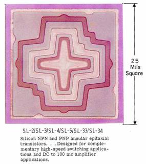
The photograph above
is from the mid 1960s, and was provided by Wilf to illustrate the silicon
transistor technology at Motorola during that timeframe. The photo is a
magnified view of an actual transistor as viewed from the top of the
wafer. The various production lines were designated “SL-X”, with each line
devoted to a specific geometry and process combination. For example, the
SL-3 line (or Silicon Line 3) produced a STAR configuration, in a TO18
package, with no gold used in the diffusion process – this was the 2N2222
line. The large darkly colored geometric boundary region around the
outside of the active transistor area in the photo above is the diffused
annular ring, which was a major Motorola innovation that prevented a
failure mode (surface inversion) which was common to transistors of this
type. By implementing such innovative processes as epitaxy and annular technology,
Motorola became a premier transistor manufacturer, competing successfully
against Fairchild and TI.
______________
|
|