|
|
Oral History – Jacques Pankove (Continued)
|
|
Another interesting adventure
happened when Fred Rosi, a materials scientist at RCA, discovered a way to
reduce the defect concentration in germanium. His improved material was
indeed much better than the standard germanium we had been using but the
high frequency performance of the transistors was seriously degraded: the
junction capacitance had increased because the indium dots had become
larger and the spacing between emitter and collector had increased causing
a longer hole transit time from emitter to collector. I speculated that
perhaps the crystal defects caused the indium dot to spread (hence high
capacitance). I quickly tested my hypothesis by using a diamond point to
damage the surface of germanium at random. Then I placed the indium dots
on the damaged areas and on the untouched areas, heated the germanium to
cause indium alloying and thus discovered that (1) the indium dots on the
damaged region penetrated deeper than on the undisturbed area and (2)
formed a smaller diameter dot. From then on RCA was able to sell improved
high frequency transistors. (J.I. Pankove, J.Appl. Phys. 28:9, 1054
(1957).
______________
Go
To Pankove Oral History, Page 5
|
|
|
Oral History – Jacques Pankove (Continued)
|
|

|
|
|
|
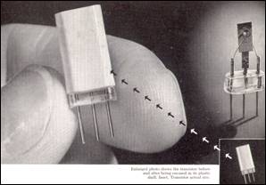
The top photo shows a very early drawing of the RCA alloy junction
transistor technology described by Dr. Pankove in the Oral History. This
photo is from a May 1952 article entitled “A Survey of Transistor
Development” written by Bob Slade from RCA. The bottom photo illustrates a
slightly later developmental version of the RCA alloy junction transistor,
from an April 1953 RCA publication entitled “Radio Age”. The
groundbreaking work that led to the development of this transistor type at
RCA is documented in the June 1952 article “Germanium P-N-P Junction
Transistor” by L.D. Armstrong, J.I. Pantchechnikoff (Pankove), C.W.
Mueller, and R.R. Law.
|
|